


NaN / 0
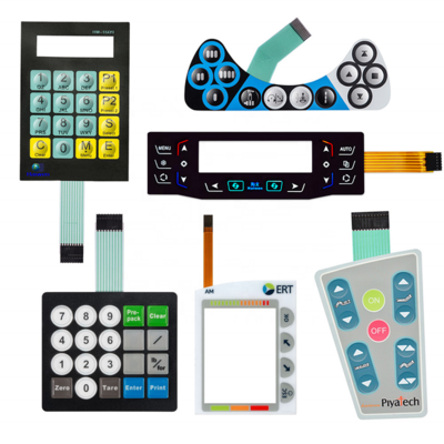
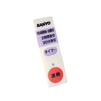
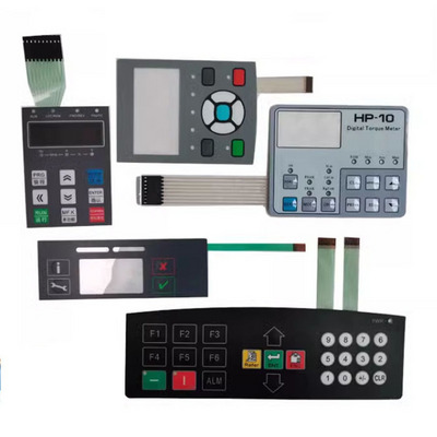
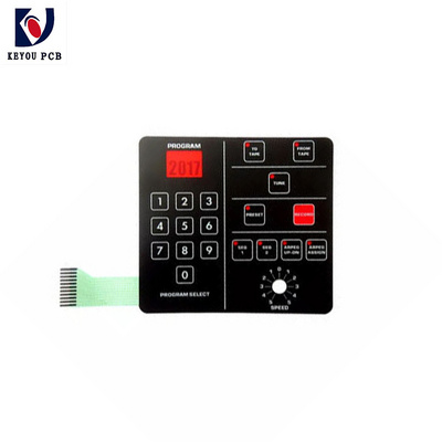
Customizing Key Pad Graphic Overlay Button Panel Membrane Keypad Keyboard Membrane Switch
Get Latest Price
US$ 3.8
≥10 Pieces
US$ 2.8
≥500 Pieces
US$ 1
≥1000 Pieces
Quick Details
Base Material:
RIGID-FLEX
Board Thickness:
0.20mm to 3.4mm
Board Size:
25*24
Model Number:
KY-FPC0015
Product Details
|
Company Capability
|
|
|
|
Layers
|
1-40 layers
|
|
|
Copper Thickness
|
0.5-6 OZ
|
|
|
Material
|
FR4 ( Shengyi China, ITEQ, KB A+,HZ),HI-TG, FR06, Rogers, Taconic, Argon, Nalco, Isola and so on
|
|
|
Solder Mask
|
green, yellow,white, blue,black,red
|
|
|
Finished Surface
|
conventional hasl, lead free hasl, immersion gold, immersion tin,immersion silver, hard gold, OSP...
|
|
|
Silkscreen color
|
white,black
|
|
|
Products Type
|
HF (High-Frequency) &(Radio Frenquency ) board, impendance controlled board, HDI board, BGA & Fine pitch board
|
|
|
Minimum line width/gap
|
3.5/4mil(laser drill)
|
|
|
Minimum hole size
|
0.15mm (mechanical drill) /4mil(laser drill)
|
|
|
Minimum Annlar Ring
|
4mil
|
|
|
Max Copper thickness
|
6OZ
|
|
|
Min Solder Mask Bridge
|
0.08mm
|
|
|
Plugging Vias capability
|
0.2-0.8mm
|
|
F A Q
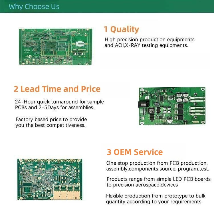
Q: What is needed for PCB /PCBA quotation? A: For Bare PCB project, please provide Quantity, Gerber file and specification like
material, surface finish treatment, copper thickness, board thickness, soldermask color and silkscreen color and other special
specs.
For PCBA project, please provide above information as well, and BOM list, pick and place file. If you need turnkey service
include programming and functional testing etc, kindly contact us for more details.
Q: Are my files safe?
A: Your files are held in complete safety and security.We protect the intellectual property for our customers in the whole
process. All documents from customers are never shared with any third parties. We are willing to sign NDA effect by customer side
local law and promising to keep customers data in high confidential level.
Q: What’s your minimum of quantity (MOQ)?
A: There is no MOQ in KEYOUPCB(PCBA shenzhen). We are able to handle small as well as large volume production with flexibility.
Q: How to calculate the shipping cost?
A: The shipping cost is determined by the destination, weight, packing size of the goods. Please let us know if you need us to
quote you the shipping cost.
Q: What other service do you have?
A: We mainly focus on PCB +Assembly +Components sourcing service. Additionally, we can also provide programming, testing, cables,
enclosure assembly service.
Q: Can we inspect quality during production?
A: Yes, we are open and transparent on each production process. We Welcome you visit our factory to inspect our production
process.
Q: What is your testing policy and how you control the quality?
A: Regarding to PCB samples, usually tested by flying probe; for PCB Volume over 3 square meters, usually tested by Electrical
fixture which is faster. As to PCBA production, there are automated optical inspection (AOI) for each batch, X-ray inspection for
BGA parts, first article inspection (FAI) before mass production.
